Thermal Stress Analysis in Multilayer PCBs
Key Takeaways
-
Multilayer PCBs have many advantages, however, multilayering puts thermal stress on a circuit board.
-
Thermal stress analysis is a temperature and stress analysis method used to determine thermal stress points in multilayer PCBs.
-
Thermal stress analysis results help PCB designers build reliable, robust, and optimized multilayer PCBs.
Thermal stress analysis can detect stress affected areas in a circuit board
Printed circuit boards (PCBs) are present in all electronic devices and are the core elements responsible for the device functioning properly. Each PCB holds an important subsystem of the device that adds to the device's features. Therefore, the more features the device has, the more PCBs the device will need to function correctly. To incorporate more PCBs into a device and to meet voltage requirements, PCBs are often layered. While there are several advantages of multilayer boards, multilayering puts thermal stress on circuit boards. That is why it is essential to conduct thermal stress analysis in multilayer boards to identify stress-affected areas and prevent thermal deformations.
Let’s first take a look at multilayer PCBs to better understand their need for thermal stress analysis.
What Are Multilayer PCBs?
To accomodate space and weight constraints in modern devices, the incorporation of multilayer PCBs is necessary. As the name suggests, multilayer PCBs consist of multiple layers of materials laminated together as a single board. Multilayer PCBs are fabricated using high pressure and temperatures to provide tight adhesion between layers and to avoid air bubbles within the board.
The Uses and Advantages of Multilayer PCBs
As modern electronics become smaller and more complex, the advantages of multilayer PCBs over single layer PCBs exponentially increase their applications in fields including:
- Data storage
- Satellite systems
- Mobile communication
- Signal transmission
- Industrial controls
- Space equipment
- Nuclear detection systems
The advantages of using multilayer PCBs for these applications include:
- Multilayer PCBs can handle more circuits than single layer or double sided PCBs within the same board area. The assembly density of multilayer PCBs makes them suitable for high capacity and high-speed applications in complex systems.
- Multilayer PCBs are small and light, which make them perfect for devices with space and weight constraints.
- Multilayer PCBs are highly reliable.
- Multilayer PCBs are flexible and are used in circuit construction where bending is required.
- Multilayer PCBs can withstand high heat and pressure and can be used in devices that require a more durable circuit.
- Controlled impedance routing is easily implemented in multilayer PCBs.
- The power and ground layers in multilayer PCBs helps EMI shielding.
Thermal Stress in Multilayer PCBs
Multilayer PCBs are formed when prepregs and core material layers are stacked up. The conductors are encapsulated within resin materials and the layers are bonded using adhesives. All the materials involved in multilayer PCBs have different thermal expansion and contraction rates, defined by the term coefficient of thermal expansion (CTE). The difference in CTE and increased temperature leads to temperature fields and thermal stress fields in multilayer PCBs. High thermal stress will cause the PCB to deform and lead to severe problems in circuit operation, reliability, and longevity.
The Importance of Thermal Stress Analysis in Multilayer PCBs
Thermal stress analysis is a temperature and stress coupled field analysis method performed on multilayer PCBs. The effect of hot and cool temperature cycles on the circuit's components and operation is analyzed using thermal stress analysis. The physical layout of multilayer PCBs is modified per the thermal stress analysis results. The layout modification helps reduce temperature fields and thermal stress fields in multilayer PCBs.
Thermal stress analysis can be helpful in many ways including:
- Component placement based on the temperature stress and shear forces placed on solder joints in multilayer PCBs.
- Predicting the chances of delamination and microcracking in multilayer PCBs.
- Predicting deformations in multilayer PCBs.
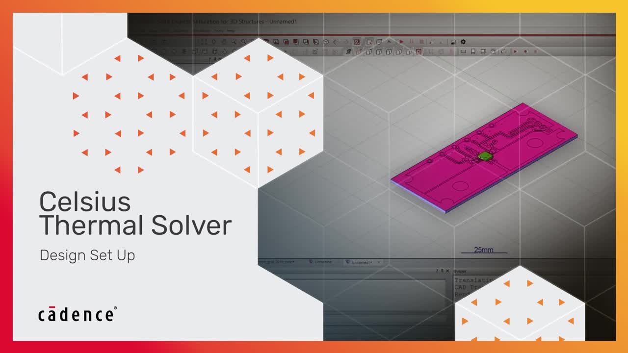
Thermal stress analysis results are useful when designing optimized multilayer PCBs. It is the most effective analysis to reduce temperature extremums and stress extremums in multilayer PCBs. It also helps achieve thermal reliability, physical board robustness, and longevity in multilayer PCBs. Cadence offers thermal stress analysis tools that increase the stability of multilayer PCBs, like our Celsius Thermal Solver featured in the video below.
Subscribe to our newsletter for the latest updates. If you’re looking to learn more about how Cadence has the solution for you, talk to us and our team of experts.