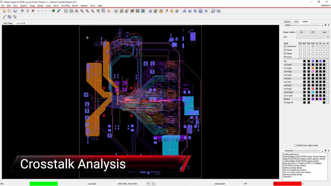
Crosstalk Analysis and Simulation in High-Speed PCB Design
Key Takeaways
-
Crosstalk analysis and simulation in high-speed design is difficult without the right field solver tools or analytical models.
-
A modern, high-speed PCB layout will need to consider single-ended and differential crosstalk as well as two power integrity problems, which can be mistaken for crosstalk.
-
With the right simulation tools, you can identify sections of an interconnect that are susceptible to crosstalk and take steps to prevent noise coupling between interconnects.
High-speed PCB design must confront crosstalk to ensure signal integrity
Today’s modern digital systems are all high-speed systems, and high-speed PCB design is no longer a specialized discipline. Low-speed protocols like SPI and I2C are not going away anytime soon, but they can’t handle the high data demands of modern computing and embedded systems. With high-speed signals comes signal and power integrity problems, as well as EMI/EMC challenges and the need for simulations to validate designs.
However, CAD tools are catching up, helping designers identify crosstalk problems and understand how parasitics play a role in determining noise coupling. If you’re experiencing crosstalk problems in your PCB layout, there are some simple solutions you can implement as long as you can pinpoint where crosstalk occurs in your PCB layout. Here are some basic things designers should know about crosstalk analysis and simulation in high-speed PCB design.
Identify Crosstalk Before Prototyping
High-speed designs with signal and power integrity problems can be difficult to debug once a design has been prototyped. Unless a designer has the foresight to place test fixtures on the board and has access to some high frequency measurement equipment, a test engineer is left to use near-field probes or contact probes to try and gather signal measurements. Simulations and some basic analysis can help a designer find locations in a design where signal integrity and power integrity problems lurk.
If you’ve prototyped a board and it continuously fails to readout signals at receivers, it’s highly probable that crosstalk is creating problems in your interconnects. Crosstalk is one signal integrity problem that can be masked by other signal and power integrity problems that create noise in high speed channels. Just to start, there are four primary areas to investigate (including crosstalk), all of which may induce noise on an interconnect. These are summarized in the table below.
|
|
Insertion loss deviation, intersymbol interference, or reflections aren’t mentioned, as these can generally be diagnosed from an eye diagram or impulse response measurement. These other sources of signal integrity problems can be investigated through complex measurements or through simulations. They are also not things that are always corrected at the interconnect design level, as newer standards (e.g., PCIe 5.0) use an equalization scheme to recover the signal at the receiver.
Because test fixtures for accurate measurements need to be designed into the board, it’s often difficult or impossible to gather in-situ measurements of a board with signal and power integrity problems. This means that modern boards need some analysis and simulation strategies to address crosstalk early in the design phase.
Fill in Gaps Using Crosstalk Analysis and Simulation in High-Speed PCB Design
Crosstalk analysis and simulation in high-speed PCB design should focus on narrowing down to the major offending pairs of nets that should be modified to prevent crosstalk. These nets can often be found in a few specific places in a PCB layout:
-
High-speed nets routed in parallel on adjacent layers
-
Single-ended nets being routed very close to differential nets
-
High-speed nets that are very densely routed
An Example With Nets on Adjacent Layers
An example of the above points is shown in the layout below. In this image, we have groups of differential pairs and single-ended traces being routed between a large FPGA and a smaller memory module. These bytelane and address traces are routed as offset striplines, but they are being routed on adjacent layers. There is the potential for strong common-mode or differential-mode crosstalk between groups of densely packed traces.
Groups of DDR address traces on two internal layers in a PCB
Let’s briefly look at crosstalk simulation results between some of the address nets in this layout.
Interpreting Crosstalk Analysis and Simulation Results
Crosstalk analysis results are rather easy to interpret: it’s simply a view of the peak value in the time-domain pulse induced on the victim net. This can be performed for multiple rise times, and the induced signal disturbance can be compared with receiver noise margins to determine if a bit error would be introduced. Here, the overshoot on net U2_HD7_AD7 is 131.4 mV, although the overlaid heat map in the PCB layout shows how this overshoot varies across the victim net.
Crosstalk simulation results
This analysis can be performed experimentally in several ways: either place groups of traces near each other with varying spacing or run multiple simulations for a single group of nets with varying rise time. This gives you a convenient way to cycle through the two main values that determine the strength of crosstalk (distance between nets and rise time of aggressor signal).
If you want to better understand coupling between these nets, you’ll want to look in the frequency domain. This can be done by taking the Fourier transform of the time-domain waveform. The alternative is to calculate the induced power spectrum directly, although this requires the use of a 3D electromagnetic field solver. The best PCB layout tools will include a specialized field solver for quickly performing these simulations.
Use the Best PCB Layout Tools With an Integrated Field Solver
When you need to perform crosstalk analysis and simulations for high-speed PCBs, you don’t need to use a complex 3D field solver. Those utilities are great for applications like EMI analysis and antenna design, but a streamlined field solver in your PCB design tools can automate crosstalk analysis directly in your PCB layout. This can give you the heat map output shown above, as well as a time-domain waveform and data table with important signal values.
When you need to perform crosstalk analysis and simulation in high-speed PCB design, use Cadence’s PCB design and analysis software with an integrated field solver that is specialized for high-speed/high-frequency interconnects. Cadence provides powerful software that helps automate many important tasks in systems analysis, including a suite of pre-layout and post-layout simulation features to evaluate your system.
Subscribe to our newsletter for the latest updates. If you’re looking to learn more about how Cadence has the solution for you, talk to us and our team of experts.