How to Use a Star Grounding Method and Why You Don't Need It
Key Takeaways
-
Star grounding is an old method of providing ground that was adapted from bench power supplies into PCBs.
-
This worked fine 50 years ago, but it is not needed today and it will create EMI problems when not used properly.
-
Using star grounding provides no benefit in electronics designs; instead, a uniform ground plane should always be used to define ground.
Grounding in electronic systems can be very complex, even for very experienced engineers. How you define and layout ground region in a PCB will influence everything from crosstalk to impedance control and generation of radiated EMI. When you start reading online guides about defining ground in a PCB, you’ll find some good and bad recommendations, and these should be carefully reviewed before you follow any advice.
One grounding method that is sometimes misunderstood and often poorly implemented is the star grounding method. This method of defining grounds for different regions and signals in a PCB can sometimes be justified, but it is no longer very useful in modern PCBs. To see why this is the case, let’s look deeper at why this might be implemented in a general electronic system. As we’ll see, a designer might make critical routing mistakes when this 40-50 year old grounding strategy is implemented in a modern PCB. Instead, a uniform ground plane should be used to support the board.
The Origin of Star Grounding
Before we look at why star grounding is not a viable strategy in today’s PCBs, it helps to look at how this method works in electronics systems. The diagram below shows a power supply connected to multiple modules. Each of these modules can be some piece of equipment that must receive power from the power supply. In this topology, the return current from each module combines at one ground connection. This just happens to be the negative terminal on the power supply.
As long as the modules in the above image are not connected to each other with any kind of ungrounded connection, then there is no problem with this arrangement. Aside from the possibility of radiated emissions being passed between modules, the various modules will not interact with each other and will not create any noise, assuming we have a perfectly decoupled, noise-free power supply.
This parallel arrangement is the standard way to connect multiple modules to a single power supply. Star grounding extends this topology onto a single PCB substrate.
Star Grounding Extended to a PCB
The image below shows how star grounding typically gets extended onto a PCB. In this diagram, we have multiple ground regions that are separated from each other and the grounds recombine back at the power supply return. The shape of each ground region could be very complex, but the point in star grounding is that the ground regions all recombine at one point, namely where the PCB connects back to the power supply.
Ground region diagram used in star grounding
This is where most designers start to implement star grounding incorrectly. To see why, let’s look at why star grounding would be used.
Why Would Anyone Use a Star Grounding Method?
The primary idea in the use of star grounding is to isolate different circuits from each other so that they do not exchange any electromagnetic energy. Because the return paths from one circuit are isolated from all other circuits, it is very difficult to couple noise between circuits. In some systems, this is a necessity, such as in audio systems, simply because it can be very difficult to track return paths at low frequencies, so it is likely that signals will interfere with each other to produce crosstalk.
At high speeds and high frequencies, where return currents closely follow the signal trace that carries them, there is no need to separate the ground plane as long as you understand how to track the return paths around your board. This is much easier at high frequencies than at low frequencies. In addition, these systems can benefit from having a very large ground plane beneath all components, as this will provide some shielding from external EMI, provide impedance controlled routing, and enable internal stripline routing where necessary.
Star Grounding the Right Way
The only correct way to use a star grounding method is to only route signals above their respective ground regions. Do not route over the gap between ground regions under any circumstances. The instant a signal travels over the gap between the two ground regions, you’ve created a return path with large loop inductance, and this loop will radiate strongly.
Successful star grounding requires only routing above the ground plane region
Connectors and Cables Across the Gap
The only time it is appropriate to route a trace across the gap is if you provide a clear return path across the gap, which would normally be done with a capacitor routed in parallel with the trace. However, this is generally a bad idea, as it will block the low frequency portion of the signal’s power spectrum, so you still have an EMI problem. Some designers will use a ferrite bead, which is an even worse idea, as this will create a resonance along the return path that will emit very strongly at mid-range frequencies.
This is why cables that are used to bridge a gap between two systems will include a grounded wire in the cable assembly. This is not just to set the ground reference potentials equal, it’s also to ensure there is a clear return path for any signals being routed across the cable. Using grounded pins and wires in connectors and cable assemblies also provides shielding against EMI. In some connectors, such as a backplane connector for very high speed signals, more than half the connectors will be interleaved ground to provide shielding for propagating signals.
Track Return Paths Over a Uniform Ground Plane
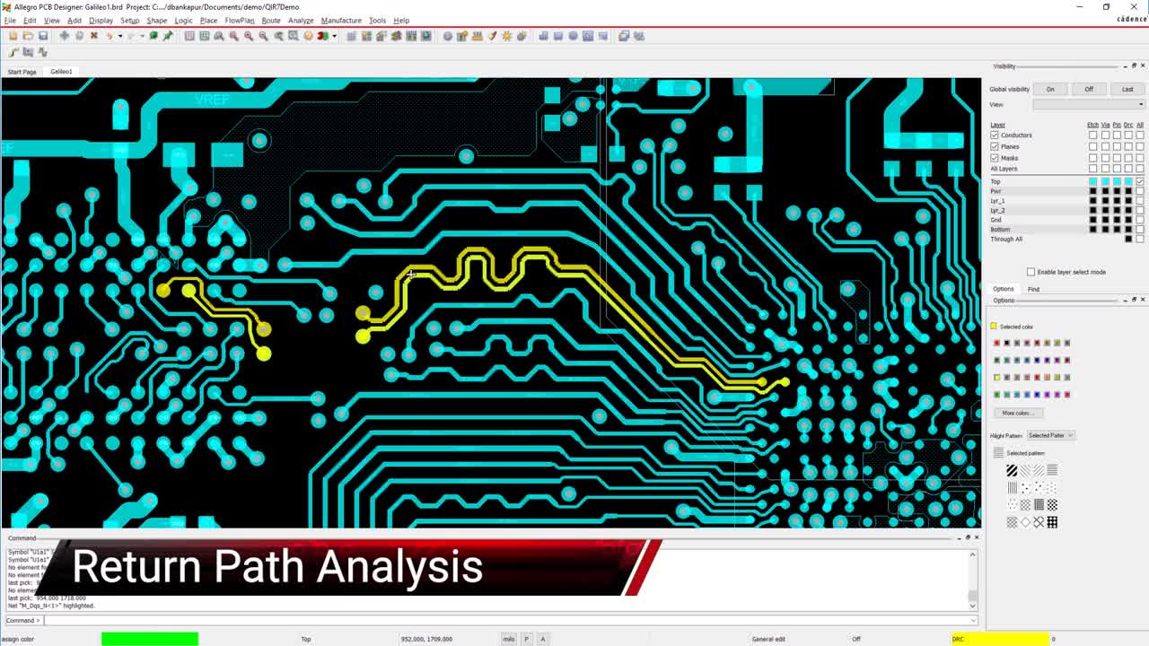
If you want to come into the modern age and eliminate all this silliness with star grounding, then use a uniform ground plane and learn to track return paths for your high speed signals. The best PCB layout software will include an integrated 3D field solver that can track the return current path in your ground plane. This will help ensure your signals cannot interfere and will eliminate the need to use old techniques like star grounding.
Cadence’s PCB design and analysis software lets you implement the best layout guidelines for modern PCBs so that you don’t need to use a star grounding method. When you use Cadence’s suite of design tools, you’ll have access to a range of simulation features you can use in PDN impedance analysis, giving you everything you need to evaluate your system’s functionality and ensure reliable signal integrity.
Subscribe to our newsletter for the latest updates. If you’re looking to learn more about how Cadence has the solution for you, talk to us and our team of experts.