PCB Trace Width Rule of Thumb
Key Takeaways
-
PCB trace width affects both current capacity and impedance, but there’s no universal rule for determining inductance.
-
Standard trace width rules use 10 mils per amp for outer layers and 20 mils per amp for inner layers, assuming 1 oz copper.
-
OrCAD X enables constraint-driven trace width design, ensuring compliance with electrical and physical design rules.

All PCB traces have some inductance, which are determined by their specific trace widths and conductor properties. While there is no specific PCB trace width rule of thumb for determining inductance, there are however formulas related to the trace impedance that can be used to determine the trace inductance. Trace inductance and impedance are interrelated — and your PCB trace width should be determined by the content of your signal, as determined by your ICs and any controlled impedance traces they may have.
PCB Trace Width Rule of Thumb for Current Capacity
|
Current (A) |
External Trace Width (mil) |
Internal Trace Width (mil) |
|
1 |
10 |
20 |
| 2 |
20 |
40 |
| 3 |
30 |
60 |
| 4 |
40 |
80 |
| 5 |
50 |
100 |
A widely used heuristic simplifies trace width selection for DC or low-frequency signals:
-
External Traces (Outer Layers): 10 mils (0.010") per amp of current.
-
Internal Traces (Inner Layers): 20 mils (0.020") per amp of current.
Assumptions Behind the Rule:
-
Copper Weight: 1 oz/ft² (35 µm thickness).
-
Temperature Rise: ~10°C above ambient.
-
Environment: Adequate airflow for outer layers (better heat dissipation than inner layers).
However, unlike current-carrying capacity, there is no simple rule of thumb for trace inductance.
A PCB Trace Rule of Thumb for Impedance
For controlled impedance traces (e.g., in high-speed or RF designs), trace width is determined by the desired impedance, which depends on the PCB stackup and trace width (dielectric material, layer thickness, etc.).
Other systems, like power converters, may not need controlled impedance along a trace, so they will typically use much larger copper with low inductance. The way to calculate the inductance is to first calculate impedance, and then use the impedance to calculate the trace inductance.
Equations for Trace Impedance in Microstrips and Striplines
The inductance of a trace can be used to calculate impedance. The inductance depends on factors like trace width, thickness, layer thickness, and dielectric properties. The bare minimum impedance model used in the PCB industry is the formula in the IPC-2141 standard. The IPC-2141 impedance equations shown below for microstrips and striplines are based on experimental observations and are reasonably accurate below ~1 GHz.
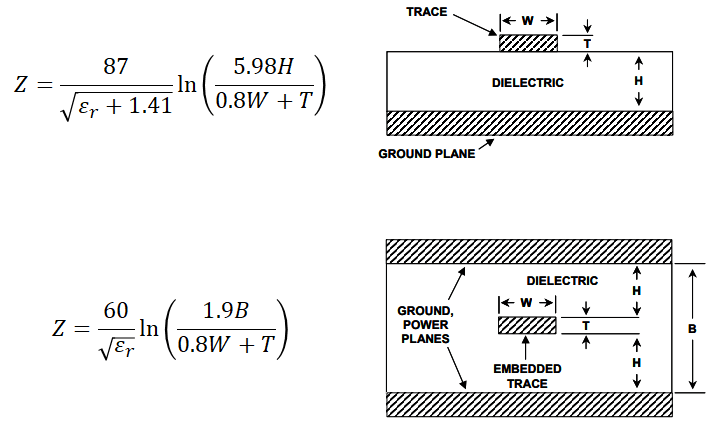
IPC-2141 trace impedance equations for microstrips and striplines.
One can show that the above equations are not perfectly accurate, as they include some assumptions that aren’t always true. In particular, the above equations are deficient in the following ways:
-
Loss tangent is omitted: All PCB laminates have some attenuation, which is quantified using the loss tangent. The loss tangent always modifies the trace impedance slightly by adding some reactance.
-
Copper roughness: The skin effect and copper roughness are lumped into the above equations and cannot be separated without a more sophisticated method (see this IEEE model for an example), so the above equations are not accurate for every fabrication process and material system.
Although the above equations aren’t perfect, they give a decent starting point for calculating trace impedance that covers cases in PCB design.
Aside: Calculating Inductance and Capacitance from Impedance
After designing the trace width to hit an impedance goal, the trace will have a specific inductance. The design process generally does not proceed in reverse, except in cases involving low-speed digital signals, low-frequency analog signals, or switching power converters that have a specific low inductance requirement. If the trace is electrically short, then you can violate the typical 50 Ohm impedance goal and design with lower trace inductance.
All this means that there is no PCB trace inductance rule of thumb. In other words, there is no specific trace inductance you should use, and there is no simple formula that gives you a PCB trace inductance for every PCB.
To see how this arises, we can again turn to the IPC-2141 equations and the constitutive impedance relation for a lossless transmission line. The IPC-2141 equations provide a capacitance per unit length equation that can be used to calculate the PCB trace inductance.
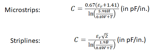
The trace capacitance is defined with respect to the nearest ground plane in the particular configuration presented above. Finally, we have two equations for the inductance of microstrip and stripline traces.
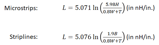
Microstrip and stripline inductance.
From this result, we see that the trace inductance depends on:
-
Trace thickness (or copper weight)
-
Layer thickness
-
Trace geometry
These factors all have to be considered together to ensure the design meets impedance goals while also determining the inductance. Generally, when calculating the inductance, we have a fixed layer thickness (H or B) and copper weight (T), and the trace width is determined in order to meet impedance and/or routing density goals. If you design a trace on one stackup with a specific laminate material, it will not have the same inductance or impedance if the same trace is placed in a different PCB stackup with different dielectric materials. If you like, you can compare inductance vs. width curves for various layer stacks.
Where the PCB Trace Inductance Rule Breaks Down
Since the above equations are logarithmic, they are only valid above a certain range of values for the geometric parameters. Whenever the argument in the above logarithms is less than 1, the result will be negative inductance. By rewriting the argument in the logarithm in terms of the ratios (W/H) or (W/B), and (T/H) or (T/B), we arrive at the following inequality that restricts the allowed trace geometry in the above formulas:
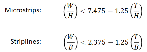
Microstrip and stripline geometry limits in order for the IPC-2141 inductance to be non-negative,
Just as an example, we can look at a simple PCB stackup with impedance control to see the microstrip inductance. For a 0.5 oz./sq. ft. copper trace on a 4-layer board with 8 mil thick dielectric and Dk = 4.2, the resulting trace width required for 50 Ohm impedance would be 15.15 mil, and the inductance would be 6.679 nH/inch. Other models will give wildly different results, which should illustrate the inadequacy of IPC-2141.
Instead of using outdated IPC-2141 formulas, there are better approaches for determining the impedance and inductance of your traces. The best PCB stackup and trace calculators will include a method of moments field solver or boundary element method field solver. These tools can be used to quickly calculate the PCB trace inductance in your board for a given stackup and impedance target. This value can then be used to determine some rough crosstalk results. Some very sensitive precision measurement designs or power converters require very low inductance routing, and these calculations can be used as a check against.
PCB Trace Width Rule of Thumb – Solved by OrCAD X
OrCAD X offers a constraint-driven design flow to control trace widths with the Constraint Manager. Engineers can define and enforce rules that automatically adjust trace widths during the routing process by utilizing Electrical and Physical Constraint Sets. The constraints can be set to either drive the design actively or function as audit checks once the layout is complete.
Electrical Constraint Sets for Trace Width Control
Electrical Constraint Sets (ECS) in OrCAD X are designed to manage electrical parameters, such as impedance and differential pair geometry. When setting trace widths, the ECS can be configured to:
-
Drive Trace Width: Automatically adjust the width during routing to maintain targeted impedance values and signal integrity. This is particularly useful when designing high-speed circuits where impedance control is critical.
-
Audit Design Compliance: Serve as a verification mechanism that checks whether the routed traces comply with predefined electrical constraints. If a trace does not meet the desired width based on the electrical rules, the system flags it for review.
Key technical details include:
-
Impedance Control: By linking the trace width to the required impedance (using the formula or tables based on the copper weight, dielectric constant, and trace geometry), designers can ensure that signal degradation and reflections are minimized.
-
Differential Pair Routing: The ECS can also manage the spacing between differential pair nets. This ensures that the pair is balanced and maintains the electrical performance criteria.
-
Automatic Rule Propagation: Any modification made to the Electrical Constraint Set propagates to all nets or net classes assigned to that set. This consistency ensures that all high-speed or sensitive signal traces meet the same performance standards.
Physical Constraint Sets and Their Role
In contrast to Electrical Constraint Sets, Physical Constraint Sets (PCS) in OrCAD X focus on the tangible aspects of trace geometry. These constraints include:
-
Minimum and Maximum Trace Widths: Engineers can specify a minimum width to ensure sufficient current carrying capacity and a maximum width to meet layout density requirements.
-
Trace-to-Trace Spacing: Physical constraints also govern the spacing between traces, which can influence the effective trace width when routing in densely packed areas or in regions with differential pairs.
-
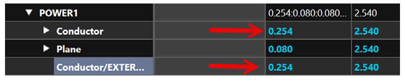
Layer-Specific Rules: Since PCB layouts may involve multiple copper layers, Physical Constraint Sets allow for layer-specific trace width constraints. This is particularly useful when different layers have varying copper weights or when routing power versus signal traces.
When setting up a Physical Constraint Set, users typically:
-
Define the Constraint Set: Create a new Physical Constraint Set within the Constraint Manager by specifying parameters such as minimum line width, neck width (for routing through tight spaces), and spacing rules.
-
Assign to Net Classes or Regions: Apply the constraint set to specific net classes or designated regions within the PCB. For example, power nets might be assigned a constraint set with a minimum trace width of 10 mils, while high-speed signal nets might have a different set based on impedance requirements.
-
Update and Propagate Rules: Any changes to the Physical Constraint Set are immediately propagated across the associated nets, ensuring design consistency and saving time during design revisions.
Integration of Electrical and Physical Constraints
One of the key strengths of OrCAD X is its ability to integrate both Electrical and Physical Constraint Sets within a unified design flow:
-
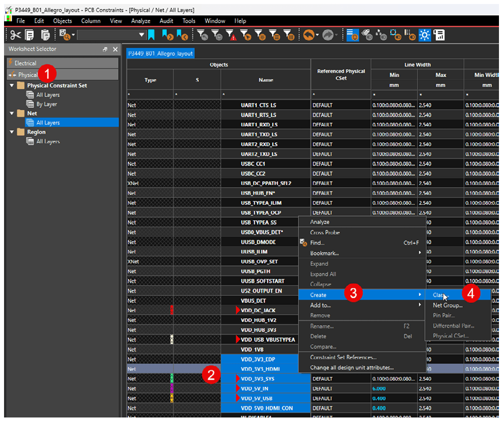
Constraint Manager Workflow: The Constraint Manager in OrCAD X provides a spreadsheet-like interface where all constraints are organized into various domains (Electrical, Physical, Spacing, etc.). This allows for easy review, modification, and assignment of constraint sets.
-
Net Classes and Groups: By grouping nets into classes (such as power, signal, or differential pairs), designers can assign a single set of trace width constraints to multiple nets simultaneously. This minimizes the manual effort required to individually adjust trace widths.
-
Real-Time Updates: As traces are routed in the PCB Editor, the constraint engine verifies each trace against the defined rules. If a trace width does not meet the criteria set in either the Electrical or Physical Constraint Sets, the system provides immediate feedback, allowing designers to correct the error on the fly.
While the PCB trace width rule of thumb offers a starting point, precision design requires more advanced tools. OrCAD X allows engineers to enforce trace width constraints based on current capacity, impedance, and spacing rules, ensuring signal integrity and manufacturability. Explore how OrCAD X streamlines PCB layout with its constraint-driven approach: Cadence PCB Design and Analysis Software.
Leading electronics providers rely on Cadence products to optimize power, space, and energy needs for a wide variety of market applications. To learn more about our innovative solutions, talk to our team of experts or subscribe to our YouTube channel.