Is There a Via Inductance Rule of Thumb?
Key Takeaways
-
All vias are basically inductors and their inductance is determined by their geometry.
-
There is no “rule of thumb” for via inductance, but there are simple formulas that can be derived from Maxwell’s equations.
-
The formula for via inductance is very simple and is the best way to determine via inductance using the via aspect ratio and PCB substrate thickness.
Do you know the inductance of these vias?
All conductive elements in a PCB have some parasitics with respect to other conductors in a PCB, and it is not always obvious what parasitics determine impedance in a PCB. Vias are placed on interconnects that require layer changes for routing, and the inductance of a via determines the via impedance. This is quite important, as the inductance of a via will dominate the via impedance at low frequencies, or when the via is very long compared to signal wavelength.
Many PCB design choices follow a “rule of thumb”, as these rules help designers quickly estimate the best geometry, layout, and routing for important plane and interconnect features in a PCB layout. The reality is that, at high speeds, rules of thumb inevitably fail, including a via inductance rule of thumb. Let’s look at how you can calculate via inductance with a simple formula and how the best design software treats interconnect impedance due to via inductance.
Don’t Use a Via Inductance Rule of Thumb
The general rule of thumb for via inductance incorrectly states that the inductance is about 2.5 pH per mil in length. However, this is only correct for a specific via aspect ratio, and this value should generally not be used. How, then, can we determine the correct inductance of a via?
As it turns out, the inductance of a via depends on two geometric factors:
-
The length of the via: In general, the inductance of a via is larger when the via is longer, but the relationship does not follow a straight line.
-
The via aspect ratio: In general, a via with larger aspect ratio has larger inductance. This relationship follows approximately a logarithmic function.
The image below shows the typical structure of a via and the formula for the inductance of a via. This formula is perhaps the most accurate formula derived for a via with negligible wall thickness, so it does not apply to filled vias.
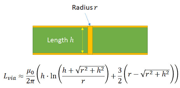
Via inductance in units of Henries.1
In the case where the aspect ratio is large (i.e., where h >> d), the above reduces to the following formula for the via inductance. Note that this formula has been rewritten in units of nH; however it's only valid if the radius (r) and length (h) are in inches:
Via inductance approximation in units of nano-Henries.
This relationship applies to any non-magnetic PCB substrate, which includes FR4 laminates. The above formula is most often used and is normally programmed into via inductance calculators found online. The next question concerns what is the desired level of via inductance, although the more important design goal is interconnect impedance.
High or Low Via Inductance?
Many engineering design choices are often framed as being “good” or “bad”, as if we always try to design for a high or low value. Via inductance can be framed in the same way, but the reality is that simply looking at via inductance is not the whole story. When designing interconnects, the important quantity is the impedance seen by signals traveling on an interconnect, as well as whether the impedance is stable throughout the signal bandwidth.
A via’s inductance, capacitance, and any parasitics will determine the impedance of a via, which will then determine how the via affects signal integrity. In high speed PCB design, we care about the following points at different frequencies:
-
Return loss: High speed signaling standards specify loss budgets, which are inclusive of return loss at vias or impedance discontinuities and insertion loss along the length of a transmission line. If a via is short enough, the input impedance at a via will be the downstream trace’s characteristic impedance and return loss will be near zero.
-
Parasitic capacitance: This allows some signal to be diverted away from the interconnect and into a nearby conductor or reference plane. In other words, some power is lost and does not reach the receiving end of the transmission line.
At low speeds/low frequencies, the via impedance does not matter so much; the input impedance along the transmission line will be close to the load impedance. At high speeds/high frequencies, the input impedance is the important quantity that will determine if a via is sized correctly. You might need to adjust the aspect ratio of the via to hit your input impedance goal.
To better understand your design, you’ll need to consider the impedance throughout an interconnect. The best PCB design software with an integrated field solver will show you the impedance of a trace along its entire length, which lets you spot excessive impedance variations due to parasitics and vias.
Don’t make bad design decisions with a via inductance rule of thumb. Instead, use PCB design and analysis software with an integrated 3D EM field solver to analyze impedance in your system. Cadence provides powerful software that helps automate many important tasks in systems analysis, including a suite of pre-layout and post-layout simulation features to evaluate your system.
Subscribe to our newsletter for the latest updates. If you’re looking to learn more about how Cadence has the solution for you, talk to us and our team of experts.
Reference:
- "Modeling Via Grounds in Microstrip" IEEE Microwave adn Guided Wave Letters, Vol. 1, No. 6, June 1991, by Goldfarb and Pucel.