How to Spot Simultaneous Switching Noise
Key Takeaways
-
Integrated circuits and PCBs all contain parasitics that can be excited by a switching digital signal.
-
All high speed digital integrated circuits can exhibit some simultaneous switching noise that is governed by parasitics in an IC structure and PCB layout.
-
Distinguishing simultaneous switching noise from another signal integrity problem requires a few simple calculations involving the inductance of your package, I/O line, and load capacitance.
The structure of modern CMOS integrated circuits creates the potential for simultaneous switching noise
Take a look at a bit stream in an eye diagram or an oscilloscope trace of a switching digital signal. When you look at the signal, you can probably pick out multiple signal integrity effects, as none of them occur in isolation. Noise from external circuits, jitter from power fluctuations, background thermal noise, overshoot, reflections, and simultaneous switching noise can all be present on a signal simultaneously. Simultaneous switching noise, better known as ground bounce, is particularly interesting, as it can sometimes be mistaken for other signal integrity problems, namely crosstalk and overshoot from reflections.
To see what actually causes this, we need to consider what happens when multiple buffers in an integrated circuit switch simultaneously (thus the name, simultaneous switching noise). The structure of integrated circuits and PCBs creates parasitics that result in strong noise when an integrated circuit switches states. To see what can happen when components switch and why we use capacitors, it helps to look at a PCB and an integrated circuit from the circuit perspective.
What Causes Simultaneous Switching Noise?
To see how simultaneous switching noise arises, we need to look at the structure of a CMOS buffer, how it connects to other CMOS buffers in the same package, and how multiple ICs connect together. In the image below, we’ve shown a typical structure of a CMOS IC with multiple buffer circuits. These CMOS buffers are all tied to the same GND net. The various buffers are switching between different states while driven by the system’s master clock. When a large number of these buffers are tied to the same GND net switch, a strong oscillation occurs that is superimposed on the desired signal level.
CMOS IC with multiple buffer circuits
Because all of these buffers are switching simultaneously, they superimpose their noise on other buffers in the circuit. When the output signal on the I/O line is measured with respect to the GND net, the resulting oscillation is clearly visible in the time domain. This should generally be measurable on an oscilloscope with an inductive near-field probe that has a high attenuation ratio.
Simultaneous Switching Noise Characteristics
There are some important points to understand about simultaneous switching noise:
- All simultaneous switching noise is caused by capacitance and inductance in the I/O transmission line, the receiver’s input capacitance, and package inductance at both ends of the interconnect.
- When more buffers are switching together, the resulting oscillation will be stronger (higher peak-to-peak voltage).
- You can’t totally eliminate this noise, but with the right bypass capacitor selection, you can get the oscillation small enough that it does not interfere with receiver components.
- The optimal case is to have the oscillation be critically damped or overdamped, but this can only practically occur with a large series resistor added on the I/O pin.
To see why these facts occur and the physical mechanism causing simultaneous switching noise, it helps to look at a single buffer circuit.
Simultaneous Switching Noise in a Single Buffer Circuit
Switching noise in a single buffer circuit occurs due to the inductance and capacitance of the I/O transmission line, load capacitance at the receiver, pin-package inductance, and any DC resistance in conductors in the signal path. The image below shows the path followed by current back to ground during an OFF to ON switching event. As we can see, the voltage loop and current path are flowing through a series LC circuit.
The path followed by the current back to ground during an OFF to ON switching event
Because the above is a series LC circuit with near zero resistance, we would expect the transient response to be an underdamped oscillation. This is standard behavior for any series LC circuit with minimal damping. These parasitics are responsible for the ringing behavior shown above when multiple buffers in a high speed digital IC switch. This is normally solved by adding a bypass capacitor across the power and ground pin of the IC and, as a result, the upward shift in the ground reference level is compensated via discharge from the bypass capacitor.
The astute designer is probably thinking “this looks a lot like crosstalk,” which is not an incorrect statement. However, this behavior might also be due to resonance on a short trace linking the two components.
Comparing Ground Bounce, Crosstalk, and Resonance
These three signal integrity effects appear to have very similar behavior when viewed on an oscilloscope trace, and they can occur simultaneously to produce complex behavior, as seen in the time domain. Distinguishing between these requires some basic calculations involving the capacitance and inductance of the interconnect.
The table below shows the expected damped oscillation frequency one might measure for each type of noise. The calculated frequency can be compared with the measured value to distinguish these noise sources in a time-domain measurement. In these formulas, Ltl is the transmission line inductance, L is the parasitic inductance in the buffer circuit, Ctl is the line capacitance, Cload is the load capacitance, tr is the signal rise time, and v is the speed of the signal on the line.
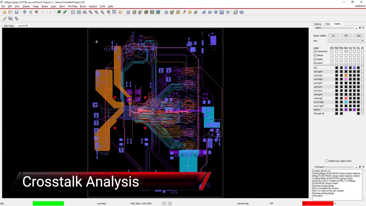
The best PCB design tools will include a 3D field solver that you can use to extract the crosstalk coupling parameters from your PCB layout. You can then use these values to determine the expected size of any voltage peak and the transient oscillation frequency in your measurements. You can also determine the time-domain response due to crosstalk directly. This is one route to help you determine whether noise in your interconnects is simultaneous switching noise, crosstalk, resonance, or some combination of these.
Advanced electronics are prone to simultaneous switching noise, and Cadence’s PCB design and analysis software can help you find and distinguish various noise sources in your design. When you use Cadence’s suite of design tools, you’ll have access to a range of simulation features you can use in PDN impedance analysis, giving you everything you need to evaluate your system’s functionality and ensure reliable signal integrity.
Subscribe to our newsletter for the latest updates. If you’re looking to learn more about how Cadence has the solution for you, talk to us and our team of experts.