The Importance of Thermal Relief in Circuit Design and PCBA Functionality
Key Takeaways
● Learn about the necessity of thermal relief in circuit design.
● Gain a greater understanding of the effects thermal relief has on the overall design.
● Learn more about the guidelines associated with thermal relief.
Thermal pads.
The element Aluminum (Al), a lightweight, silvery-white metal of the principal Group 13 (boron group) of the periodic table, finds itself widely utilized. However, most recognize it in the form of aluminum foil since it is such a staple in today's kitchens. That's because chefs of all levels understand how the right temperature makes all the difference.
From the time of the Roman Empire to the present day, we can trace evidence of the element's unique heating and cooling properties. Its ability to manage and conduct heat is what affords this element widespread utilization. In the fields of PCBA and electronics, designs themselves pivot on a design's ability to regulate temperature properly. What we call thermal relief is paramount to performance, functionality, and lifecycle.
What Is Thermal Relief?
In the area of PCBA, managing and conducting heat is essential to a circuit board's overall design success. Nearly all PCBs utilize large areas of metal for ground planes or power planes, and these planes will generally connect to numerous component pins. When these pins are the leads for a thru-hole device, unsoldering or soldering these pins can pose a high level of difficulty with the significant amount of metal in the planes. This brings about the need for thermal relief.
Thermal relief for a PCB comes in the form of a thermal relief pad or thermal pad. These thermal relief pads are PCB pads that are connected to a copper pour using a thermal connection. Whether your PCB design is a simple single-sided board or an intricate multi-layer board, there will usually be some significant areas of metal on it for power conduction and ground. The metal can be a network of traces, or maybe a sizable, filled power plane.
In either case, the additional metal will behave like a heat sink for the connected pin, thus producing soldering issues such as:
-
In regards to SMT component pins, these issues typically arise with smaller SMT components when soldering one of their pins directly to a large area of metal. This imbalance in the metal between the pins creates a tombstone effect, which is the result of the solder melting faster on one side than the other.
-
In the case of thru-hole components, their pins can suffer from inadequate heat levels to support proper soldering, which can result in a cold solder joint. Furthermore, attempting to unsolder thru-hole components directly soldered to significant areas of metal will result in the application of excessive heat, resulting in possible PCB, trace, and component damage.
Other Thermal Relief Considerations
A board's design dictates the component connections to these broad areas of metal for necessary functionality.
One other exacerbating issue is that a design's requirements typically include as much metal as possible to accommodate the PCB's electrical demands.
And, to facilitate increased current loads and enhance power integrity, power nets also require this metal. As you might imagine, this creates a dichotomy between electrical performance and standards of manufacturability. However, this is where thermal relief can provide a much-needed compromise.
PCB Thermal Relief Guidelines
-
If connecting a thru-hole pin to a power plane, fill of metal, or metal that is wider than the component's pad, use thermal relief pads.
-
Utilize thermal relief between a solder pad and the area it is soldered to if SMT components are soldered directly to broad areas of metal.
-
Correlate your width and spoke count of your thermal relief with that pins power conduction level. For example, if its power requirement is a minimum trace width of 30 mils then your thermal relief pad should have 30 mils of spokes (i.e., three spokes each at 10 mils wide).
-
Ensure that you follow CAD system rules for your thermal relief pads and provide your setup accordingly.
-
There are times you will encounter spoke connectivity issues. In general, these issues include congestion, use in split planes, and spacing issues. Therefore, be sure that your software is set up for and can identify minimum thermal relief connections.
In 1597, Sir Francis Bacon coined the phrase," Knowledge is power." This expression is as true today as it was then. Therefore, the best way to address thermal reliefs in your applicable designs is through an increased understanding and knowledge. You cannot overstate the importance of thermal relief in circuit design, nor should you overlook it.
So, be sure to enlist the assistance of one of your company's greatest assets--your contract manufacturer. Be sure that your CM has the necessary experience in building the types of PCBs that match your company's needs. With heat management and thermal relief being vital to circuit design, ensure your CM understands the intricate details of proper thermal relief.
A PCB with multiple thermal pads.
Thankfully, with our PCB Design and Analysis overview page, you will be sure to have your designers and production teams working together towards implementing proper thermal relief for all of your company's applicable designs and manufacturing needs.
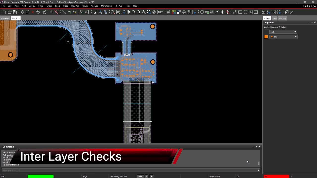
Whether you are utilizing a single-sided board or a multi-layer design, you will need the right set of PCB layout and design software. Allegro PCB Designer, and Cadence's full suite of design tools, can help you create designs from verified component models and analyze all aspects of their functionality. You'll also have access to a set of tools for MCAD design and preparing for manufacturing.
If you're looking to learn more about how Cadence has the solution for you, talk to us and our team of experts.