What’s the Difference Between Stray and Parasitic Capacitance?
Key Takeaways
-
Stray capacitance and parasitic capacitance refer to the same basic idea, but the terms are sometimes used to describe different situations.
-
All designs will have some stray or parasitic capacitance, but they may not be noticeable in some designs.
-
Understanding where this unintended capacitance arises will help you explain the bandlimited behavior of real high-speed/high-frequency channels.
Density between traces in a PCB creates stray and parasitic capacitance
When you think of terms like “stray capacitance” or “parasitic capacitance,” it’s easy to wonder how they might be different. These terms are sometimes used interchangeably, which can make it even harder to understand the difference between stray and parasitic capacitance. PCB designers prefer one while integrated circuit designers prefer another, but both terms refer to the same effect in an electronic system.
With both groups of engineers muddling terminology, new engineers might get confused when these terms are thrown around. If you’re a new designer, let us help clear up the difference between stray and parasitic capacitance.
There Is No Difference Between Stray and Parasitic Capacitance
These two terms refer to the same effect in an electronic system: the natural capacitance that exists between two conductors that are separated by free space or a dielectric. If you think back to your electromagnetism 101 class, you might remember those hypothetical problems where you need to calculate capacitance between two arbitrarily shaped conductors.
Any two conductors that are separated by a dielectric form a capacitor. It doesn’t matter if these conductors happen to be placed on a semiconductor wafer or if they are traces and planes on a PCB. If you look at certain components (such as coils) or the surface of a typical PCB, it’s easy to spot some pairs of conductors that will have some capacitance.
Two arbitrary conductors that are separated in space will balance each other with equal and opposite charges when brought up to some arbitrary potential, forming a capacitor
We can all this capacitance “stray capacitance” or “parasitic capacitance”, as there is no difference between these terms. Some designers prefer one term over the other, but they are both describing the same structural property of an electrical system. Although these two terms describe the same electrostatic effect, not all designers use them interchangeably.
Stray Capacitance
The term “stray capacitance” is sometimes used to describe the unintended capacitance within a component, such as capacitance between windings in a coil or between conductors in an integrated circuit. As an example, consider the inductor coil below. The windings in the coil are separated by some distance, which determines the capacitance between windings in the coil.
There is some stray capacitance between the windings in an inductor coil
Similarly, on the input to an IC, there is some capacitance between the input lead and the internal ground plane on the semiconductor die. This is normally called “load capacitance” in a component datasheet, and this load capacitance will determine the rolloff and rise time in the voltage seen at the input buffer on the IC.
Parasitic Capacitance
This term is often used to describe the unintended capacitance seen in a PCB layout, where the capacitance arises between planes, traces, vias, and other conductors that make up the circuit board. For example, when looking at the cross-section of an interconnect and its nearby plane layers, we can see some clear locations where parasitic capacitance arises, as shown below.
Parasitic capacitance is also found alongside parasitic inductance
The savvy designer will notice that parasitic capacitance is unavoidable, and it actually determines transmission line impedance, PDN impedance, via impedance, antenna impedance, and any other impedance for printed components. The effects of parasitic/stray capacitance span beyond determining impedance, and it is used to explain many effects that happen in a PCB.
The Effects of Stray and Parasitic Capacitance
The main effect of stray and parasitic capacitance is to produce measurement errors in an interconnect, component, or other area of an electrical system. Measurement errors can occur through many different mechanisms, especially in complex systems like PCBs. Some of these effects include:
- Bandlimiting: Parasitic/stray capacitance acts like a high-pass filter, which creates rolloff in a transmission line transfer function or components like resistors.
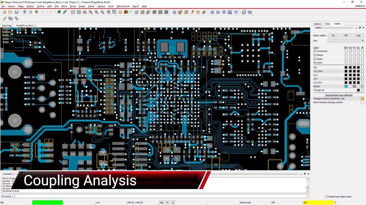
- Coupling: In general, this refers to the ability for a signal to pass from one conductor to another unintentionally. For example, capacitive coupling creates crosstalk between traces.
- Impedance modification: This is related to bandlimiting and coupling. Stray/parasitic capacitance will modify impedance by producing a displacement current in nearby conductors.
From a circuit perspective, stray/parasitic capacitance acts like an unwanted capacitor along an interconnect or in a circuit. This explains the bandlimiting behavior; the function of parasitic capacitance is to filter some signal away from an interconnect or circuit, and this increases at higher frequencies, creating low-pass filter behavior.
When you need to determine stray or parasitic capacitance in your PCB layout, you’ll get the most accurate results when you use PCB layout software with an integrated 3D field solver. These tools give you the ability to calculate parasitics in a complex, arbitrary structure like a PCB layout, integrated circuit layout, or other complex system.
If you’re designing high-speed/high-frequency electronics, you’ll need to identify parasitics in your physical layout to ensure power and signal integrity. Cadence’s PCB design and analysis software can help you locate stray and parasitic capacitance in your design and experiment with ways to reduce parasitics in your PCB layout. When you use Cadence’s suite of design tools, you’ll have access to a range of simulation features you can use in PDN impedance analysis, giving you everything you need to evaluate your system’s functionality and ensure reliable signal integrity.
Subscribe to our newsletter for the latest updates. If you’re looking to learn more about how Cadence has the solution for you, talk to us and our team of experts.