What Is the Loop Inductance of a Transmission Line?
Key Takeaways
-
All transmission lines can be described with a circuit model, where parameters are determined from Maxwell’s equations.
-
The loop inductance should be examined in long and short transmission lines to understand EMI, propagation behavior, and return paths.
-
Numerical tools can be used to determine the inductance of PCB transmission lines.
Just like this foil inductor, your transmission lines have some loop inductance
Generally, when we talk about the inductance of a trace or a transmission line, we talk about it in terms of crosstalk. This is a universal aspect of any trace, meaning the self-inductance and mutual inductance of a trace will determine how noise and power are induced in a victim trace from some external noise source. When we start to think about transmission lines, there are additional concepts needed to understand how inductance influences the electrical behavior of propagating waves.
When designing transmission lines to meet a design impedance value, as well as when trying to ensure low crosstalk and EMI, it’s important to understand the loop inductance of a transmission line and its relation to the return current. With the right design tools, you can plot the return current path in your PCB layout, IC layout, or other electronic system. This will help you identify potential EMI problems due to large loop inductances.
How the Loop Inductance of a Transmission Line Affects Electrical Behavior
All circuits are formed as closed loops of conductor and components, and we like to state that currents follow closed loops in any electronic system. While current does not move through a big circle like water in a pipe, there is active motion of charge within a specific region of conductor, which forms a closed loop. Anytime we have a structure that supports closed-loop motion of charge, the closed-loop structure formed by the current path has some inductance.
How Loop Inductance Is Formed
The loop current does not form a literal circle, but rather exists within a region in the system that has the lowest inductance. This is easiest to see in a PCB with a single-ended transmission line being routed over a gap in a ground plane. In the image below, a trace is being routed over two separate ground planes, and a capacitor is used to remove any DC voltage offset between the planes and create a uniform ground.
A trace is routed over two separate ground planes and a capacitor is used to remove any DC voltage offset between the planes and create a uniform ground
The return current in this situation must follow the path of least inductance, which is through the capacitor and back along the trace. Obviously, there will be some current distribution, and the current will not follow these straight lines. However, this nicely illustrates how a loop is formed by the return current. This loop has some inductance, which contributes to the total loop inductance of the incoming transmission line. We can draw the same type of picture for many other transmission lines in PCBs, ICs, or power systems.
Differential Pairs
It is often said that differential pairs do not have a return path, which is not true. The return path is defined by the reference plane near the pairs and the distance between the two pairs. The return path between two pairs also creates some loop inductance, which can receive crosstalk as differential mode noise. This is one reason to always keep a ground plane below differential pairs; it reduces the field strength from other traces seen between the two sides of a differential pair and thus reduces received EMI.
Why Identify the Loop Inductance of a Transmission Line?
When there is large loop inductance due to a poorly defined return path, there are some important, undesired effects that will occur:
-
Inductive crosstalk: This type of crosstalk occurs due to high loop inductance, which leads to higher mutual inductance between two traces.
-
Radiated EMI: When current flows in a larger loop, it generates more magnetic flux, and there is a greater chance that magnetic flux will induce an unwanted current somewhere outside the system. This is one major reason that many products fail to pass EMC testing.
-
Impedance discontinuity and reflection: A section of transmission line with a large loop inductance will have large impedance in that section, so there is a chance for power loss due to reflection.
These points should illustrate the necessity of always routing transmission lines with well-defined return paths. If you can calculate the loop inductance of a transmission line and plot its return path, you can have greater assurance that the line will not create EMI problems.
Use a Numerical Field Solver for Impedance and Return Path Calculations
In principle, you can calculate the inductance of a trace with a 3D field solver utility, but this is not the norm in transmission line design. Instead, field solvers normally focus on impedance and calculating the current distribution around the trace. The former is needed to ensure power transfer between transmission lines and components with desired system impedance, while the latter is just the return path for current that forms the loop inductance.
If you know the impedance and the Dk value seen by signals traveling on the trace, you can calculate the loop inductance of a transmission line:
Loop inductance of a transmission line
Note that this ignores losses due to skin effect and DC resistance, it ignores parasitics, and it’s only valid at individual frequencies. This is one reason to use a field solver to get accurate impedance values, which can then be used to calculate loop inductance.
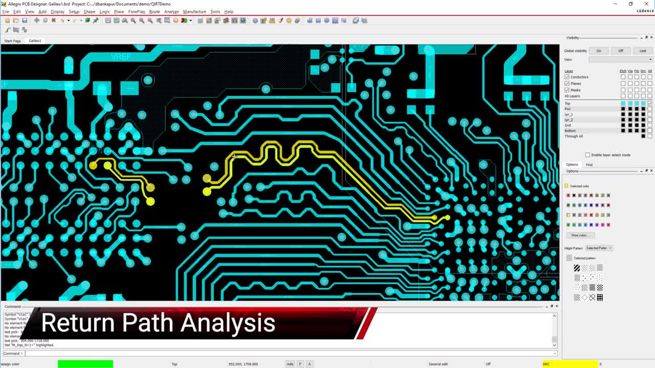
Field solver utilities can determine the impedance of a transmission line along each section. The example shown here is for a group of DDR transmission lines in parallel
If you’re worried about return path tracking, the best utilities can calculate the return current density distribution directly. You won’t have a specific loop inductance value, but you will be able to see when the return diverges and forms a very large loop inductance. You can then focus on re-routing signals and redesigning ground planes to ensure the design has low loop inductance return paths associated with your transmission lines.
When you need to solve problems associated with the loop inductance of a transmission line, make sure to use PCB design and analysis software with an integrated 3D EM field solver and a complete set of CAD tools. Cadence provides powerful software that helps automate many important tasks in systems analysis, including a suite of pre-layout and post-layout simulation features to evaluate your system.
Subscribe to our newsletter for the latest updates. If you’re looking to learn more about how Cadence has the solution for you, talk to us and our team of experts.